
- About the Journal
- Editorial Board
- Review Process
- Author Guidelines
- Article Processing Charges
- Special Issues
- Current Issue
- Past Issue
 Current Research in Materials Chemistry
Current Research in Materials Chemistry Volume 3 (2021), Article ID: CRMC-111
https://doi.org/10.33790/crmc1100111Research Article
Low Temperature Reactive Flux Growth of SiC and SiC-AlNusing Al-Si Flux
N. B. Singh and Raghaw S. Rai*
Department of Chemistry and Biochemistry, and Computer Science and Electrical Engineering University of Maryland, Baltimore County, Baltimore, MD 21250, United States.
Corresponding Author Details: Raghaw S. Rai, Department of Chemistry and Biochemistry, and Computer Science and Electrical Engineering University of Maryland, Baltimore County, Baltimore, MD 21250, United States. E-mail: singna@umbc.edu
Received date: 17th March, 2021
Accepted date: 22nd July, 2021
Published date: 24th July, 2021
Citation: Singh, N.B., & Rai, R.S. (2021). Low Temperature Reactive Flux Growth of SiC and SiC-AlNusing Al-Si Flux. Cur Res Mater Chem 3(1): 111.
Copyright: ©2021, This is an open-access article distributed under the terms of the Creative Commons Attribution License 4.0, which permits unrestricted use, distribution, and reproduction in any medium, provided the original author and source are credited.Creative Commons Attribution License, which permits unrestricted use, distribution, and reproduction in any medium, provided the original author and source are credited
Abstract
Al - 12% Si alloy system was used as nutrient flux to grow silicon carbide at low temperature by reactive flux growth. Thick films were grown below 900°C on a SiC substrate having Al-Si melt rotated with a speed of 30rpm in a graphite cruciblein nitrogen atmosphere. A constant 2 atmospheric pressure of nitrogen was used on the melt. Using longer soak time of the melt in the presence of carbon impurity, the destruction of dendritic morphology was observed that subsequently resulted into the formation of cellular, colony and facetted crystal morphology. Photoluminescence data from film showed SiC with higher band gap in the presence of aluminum nitride.
Keywords:
A1.Crystallites; A1. Nucleation; A1. Optical morphology; A1.Solidification; A2. Growth from melt; B2.Semiconducting silicon compound;
Introduction
Silicon carbide is an important material for the high power and high temperature electronics, RF, and radiation hardened devices and components. It has been developed and used as a substrate [1-5] for the Ga Nepitaxial growth as well as for a variety of high electron mobility transistor (HEMT) and other devices [6-8]. However, application of SiC as a substrate material for GaN has been less than perfect due to different crystal structure, the formation of different polytype structures in SiC that cause defects in the film and other problems including changes in properties such as mobility and bandgap. Thin layer of AlN has been extensively used as the buffer layer on the SiC wafers to avoid crystallographic problem of different polytype structures. Several other substrates like β-Ga2 O3 and GaN are still under development. The, thermal conductivity and heat capacity of these substrates are orders of magnitude lower than SiC. The low thermal conductivity substrates are alright for the light emitting diodes (LEDs), but not good for high temperature high power components where better thermal properties for fast heat dissipation is required. Modelling and experimental results have demonstrated [9] that 2H-SiC has higher conductivity, mobility, larger bandgap and refractive index [10] compared to the other polytypes of SiC. Growth of 2H-SiC has not been achieved at growth temperature >1700°C, which is typically used incommercial method of physical vapor transport for 4H-SiC and 6H-SiC substrate production. It has been demonstrated by earlier researchers [11-[15] that even a small composition of aluminum nitride in silicon carbide matrix produces 2H-SiC structure. The phase diagram studies on AlN-SiC [16] shows 2Hstructure for a very large composition range and a pioneering study by Burton et al [17] explained that ease with which homogeneous solid solutions and 2H- single crystals can be synthesized. The physical vapor transport growth for pure AlN and SiC requires very high temperature [18-20] in addition to the problem of reaction between source material and crucible. Kawamura etal. [21] have used lithium flux to grow of 2H-SiC at low temperature. This study has two objectives: (1) evaluate suitability of Al-Si flux by addition of carbon to grow 2H-SiC below 1000°C and (2) transition of morphology due to enhanced reaction by the addition of carbon in dynamic condition.
Experimental Methods
2.1 Source Material:
The Al-Si alloy was used as the flux and source material for the Aluminum and silicon. The composition was Al – 12% Si with varying amounts of carbon (1-5)%. Al and Si materials were listed for 99.999% purity, and graphite powder (99%) was used as the carbon source. We used nitrogen and a very low amount of aluminum nitride in the melt.
2.2 Crystal Growth Conditions:
The crystal growth furnace for the reactive flux growth is shown in Figure 1. The design is very similar to the liquid phase epitaxial growth. Al-Simelt was contained in a graphite crucible under a nitrogen atmosphere. The temperature of the furnace could be raised up to 1200°C with a 220 Volt Athena controller. The furnace was designed to translate in the range of 1cm/ day to 30cm/day with the help of two gears attached to platform containing seed holder. Also, the seed holder box could be moved with hand to adjust the height without attaching with motor. Temperature was raised to 900°C for each run and held for four hours. The melt was stirred with asmall SiC wafer at the speed up to 30rpm to provide uniform mixing.
A nitrogen atmosphere was used in the furnace enclosure to minimize the oxidation of the melt. After four hours of mixing the melt was cooled at two different rates (4.63 x 10⁻³ K/s and 2.19x 10⁻³ K/s). In the typical experiments, we lowered the temperature up to 8750C.

Figure 1: Custom furnace for reactive flux growth containing ceramic insulation and 4 3”diameter thick wall graphite crucible.
2.3 Characterization of Solidified Material:
The grown thick film on the SiC substrate was studied for its morphology by optical microscopy, Scanning electron Microscope (SEM), Auger and composition by Energy Dispersive Spectroscopy (EDS). Microstructural evolution studies were carried out on the casted sample on a SiC substrate by investigating the morphological changes in α-Al and Si phases due to changes in solidification conditions and carbon impurity. To study the morphology, we used the as-grown material followed by etching with a dilute solution of HF+ HNO3 + H2O. Photoluminescence studies was performed to determine polytype structures of the grown film.
Results And Discussion
Early attempts to achieve 2H- multi- and poly crystalline alloys were obtained in SiC-AlN alloys [11-15] by hot-pressing. It generally involves high temperatures in the range of 1700-2100°C. Results of Zangvil and Ruh [16] showed the existence of a flat miscibility gap at 1900°C, above which a 2H solid solution of SiC-AlN could be achieved. The miscibility gap thus poses difficulties for the growth of SiCAlN alloy films by conventional techniques at lower temperature. Burton and his coworkers [17] proposed excellent mechanism for the solid solution formation and development of wurtzite structure for a large range of composition. Using physical vapor transport and high temperature, Edgar and his coworkers and others [18-20] performed growth of solid solutions. To avoid the reactivity of crucible at high temperature, Kawamura et al. [21] have employed an innovative approach of flux growth using lithium as a flux to grow 2H-SiC. Lithium formed the metastable and several compositions of less stable carbides. They showed that in the temperature region above 1000°C, 3C-SiC is achieved. 4H-SiC and 6H-SiC phases are grown above 1750°C. In the temperature range of 800°C the transition to 2H-SiCoccurred [21] when they used lithium as a flux to grow SiC single crystals. The biggest problem in this case was hardening of lithium-based carbides. Material used to get very hard and stick in the crucible in very short time near 800°C growth temperature. In this study, we evaluated low temperature aluminum-silicon and indium fluxes to grow crystals below 900°C. As mentioned in the experimental section, the growth design was very similar to the liquid phase epitaxial growth process.
Several SiC wafers were cut in the size of nearly 2x5 cm and 370 μm thick and were used to stir the melt and film growth. The rotation rate of 20-30 rpm was used for stirring and growing the film on the substrate. For mixing at early the stage, slightly higher rotation than 30rpm was used. For the growth, two solidification rates were used after soaking the melt at 900°C. The cooling rates used were 4.63 x 10⁻³ K/s and 2.19x 10⁻³ K/s. To optimize the soaking period and understand the etching of the seed SiC, the growth run was stopped after 15 minutes at the early stage of this study. Figure 2 shows the microstructure of at the slower growth rate of the aluminum rich Al-Si alloy. These aluminum rich dendrites show mainly primary and secondary branches, but tertiary branches were not observed. It was observed that secondary branches are at nearly 90 degrees from the primary branches, indicating strong anisotropy. Further, the dimension of the secondary branches, especially the width, was very large. Also, some substructures were observed in the secondary branches. Between each dendrite, there was an Al-Si eutectic liquid which enhanced the coarsening of the dendrites. Darker regions are carbon coming from the crucible.

Figure 2: Morphology of α-Aluminum dendrites. Darker region shows liquid and some carbon impurities coming from the crucible.
A faster cooling and quenching rate of the melt compared to rates mentioned above for crystal growth produced dendritic and cell structures side-by-side. Figure 3 (a) and (b) show the morphology of the dendrites and cells where sizes of the cells are very large. In the transition area, elongated cells, which subsequently broke into many other cells, were observed. This was observed when mixing was not complete. For this reason, in most cases the melt was mixed for four to six hours. The aluminum reacted with the graphite crucible and showed the segregation of the carbon addition. As the aluminum and silicon react with the carbon, they form aluminum carbide and silicon carbide. However, supply of carbon just by reaction with the crucible wall is very slow and additional powdered graphite was added to ensure carbide formation during soaking period at 900°C.
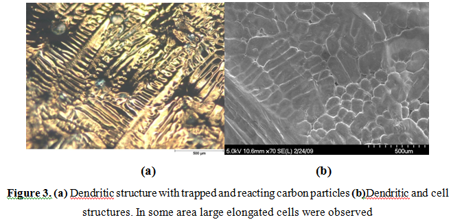
Figure 3:(a) Dendritic structure with trapped and reacting carbon particles (b)Dendritic and cell structures. In some area large elongated cells were observed

Figure 4. (a) Early stage of dissolution of carbon from crucible in Al-Si alloy and (b)Composition shows dissolution of carbon in 30 minutes in Al-Si alloy.
Carbon coming from the crucible started dissolving in the Al-Si alloy after 30 minutes. However, small addition of powder speeded dissolution immediately after addition into the Al-12%Si melt. Figure 4 (a) shows the carbon dissolution and reaction with solvent after 10-15 minutes of addition of carbon. The EDS spectrum from area A2 is shown in figure 5 (b) after carbon dissolution and 10-15 minutes of deposition during stirring. It shows, Figure4 (a), trapping of particles as well as a large concentration of carbon (dark and precipitate region). The magnitude of coarsening increasedand, in some cases, growth of secondary dendrites (arms) slowed down. With continuous stirring, dendrites changed completely into spherulitic structures (Figure 5) where the nucleus has very large concentration of carbon. Figures 5 show different stages of the dissolution and structure formation closed to the carbon particle. Figure 5(b) shows that the dissolution of carbon creates a huge concentration gradient, modifies the morphology, and generates colony type microstructures. Despite stirring, the alloy retains some dendritic morphology far from the high carbon concentration. Secondary branches which appeared at the early stage of carbon dissolution, disappeared with increasing carbon concentration in alloys the concentration of carbon caused spider like microstructures around the dissolving carbon particles. With an increasing concentration of carbon (above 3%), the dendritic or any other ordered structure starts continuously disappearing.

Figure 5.(a) Dissolution of carbon creates huge concentration gradient, but alloy retains some dendritic morphology far from the high carbon concentration and (b)Colony structures around carbon particles
Figures 6 show the morphology of deposited material on the wafer (a) showing uniform growth and (b) a different region of the substrate showing faceted morphology. Large size crystals (mm size) were observed on the top of the frozen melt by slow cooling Si-Al flux containing AlN and carbon in the graphite crucible. The nucleation of faceted crystals started on the substrate after reaction with carbon.
It grew in several layers like graphite and then transformed into multi-layered hexagons on the silicon carbide substrates. As it was mentioned earlier in this section, the melt is kept several hours for soaking before cooling. Typically, the melt was cooled 50K in 8-10 hours. For uniform deposition, it was found that a cooling of 25K in 30-48 hours was required.
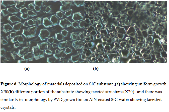
Figure 6. Morphology of materials deposited on SiC substrate,(a) showing uniform growth X50(b) different portion of the substrate showing faceted structures(X20), and there was similarity in morphology by PVD grown fim on AlN coated SiC wafer showing facetted crystals.
As the growth progresses, hexagons and facetted steps merge and morphology changes to that shown in Figure 7. As seen in Figure 8 hexagons are stacked on the top of the other hexagon. The stacked hexagons change into large-layered materials growing on the top of the other layers without visible micro holes typically observed in the case of pure SiC growth. In many cases, hexagons grew on the top of each other and made multi-layer before expanding on the substrate. Laterally, these hexagons merge and form large single thick film, but growth steps are clearly visible as shown in Figure 8. This demonstrates that hexagons coarsen and merge to form cm size grains. For the two- dimensional thick film growth in presence of AlN or on the AlN interface the mechanism of charge neutrality (mixed interface) has been discussed for the growth of solid solution by Burton et al. [17]. They indicated that for AlN-SiC composites and solid solutions, SiC is deposited on N-rich terminals followed by Wurtzite 2x2 reconstructions with N-atom. It also supports the finding of other researchers [11-16] that AlN solid solution grains inhibits the growth of the 6H-SiC grains since AlN(2H) will not go into solid solution in the SiC(6H) structure and effectively creates Wurtzite structures in composites.

Figure 7. Thick filmdeposited for a period of 48 hours. Thickness was larger than 350 μm. (b) layered structures similar to Figure 1(b) of Kawamura (21) x 20
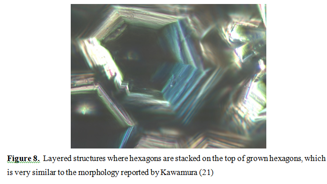
Figure 8. Layered structures where hexagons are stacked on the top of grown hexagons, which is very similar to the morphology reported by Kawamura (21)
Detailed studies [22-25] of samples, grown by PVD, CVD and low temperature CVD using hexamethyldisilane (HMDS) based growth, characterization by SEM, TEM and other techniques of the samples grown on 6H-SiC (AlN/SiC) substrateindicate the nucleation and interface diffusion. This study revealed that interface between the substrate and grown film was diffused. High resolution TEM was performed to evaluate the film grown on 6H-SiC substrate. Figure 9(a, b) shows TEM images where rough and stepped interface is seen between grown film and substrate in the lower magnification image of Figure 9 (a). A darker contrast seen inthe high resolution TEM image, Figure 9 (b),having a periodic structure of ~15 Å corresponds to 6H-SiC in the substrate region and lighter region with a periodic pattern of ~5 Å corresponds to 2H-SiC in the film region. This TEM data confirmed that grown film is 2H-SiC, which is consistent as significant amount of AlN was mixed in the source material.
These films were further characterized by photoluminescence to evaluate the bandgap energy and compare with the reported values for 6H-SiC and 4H-SiC. Figure 10 shows results of the photoluminescence data for two different samples grown in two different conditions. Both samples showed identical peaks for 2H-SiC at identical position indicating bandgaps of materials. However, intensity differed significantly. Also, it appears that samples showed slightly higher values of bandgaps of each material. As shown in Figure 10(a) there was no peak of 6H-SiC whereas Figure 10(b) shows a very weak peak of the 6H-SiC polytype.
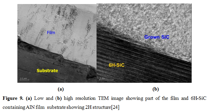
Figure 9. (a) Low and (b) high resolution TEM image showing part of the film and 6H-SiC containing AlN film substrate showing 2H structure [24]
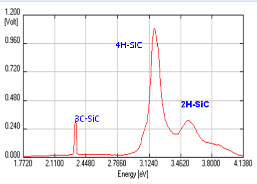
Figure 10.(a)
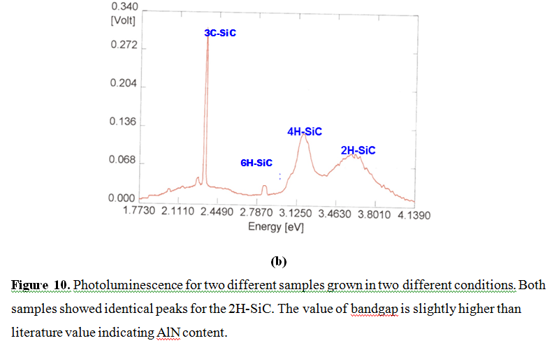
Figure 10.(b) Photoluminescence for two different samples grown in two different conditions. Both samples showed identical peaks for the 2H-SiC. The value of bandgap is slightly higher than literature value indicating AlN content.
These data also support findings of Kawamura et al. [21] that a low temperature growth favors 2H-SiC polytype formation. In addition, growth by reactive CVD using HMDS on SiC film containing extremely thin AlN film [22-26] favors polytypes with higher bandgap materials on SiC and Si substrate coated with thin AlN film. It was observed that the application of Al-Si melt method also suffers due to hardening of the solid very similar to the lithium flux method reported by Kawamura et al. [21]. The effort to solve this hardening problem of flux is underway.
Summary
Al - 12% Si alloy flux was used as nutrient flux to grow silicon carbide at low temperature by reactive flux growth. Reaction occurred by the dissolution of carbon in the melt under dynamic conditions. The material was nucleated on a SiC substrate while the Al-Si melt was rotated with a speed of 30rpm in a graphite crucible. A constant nitrogen pressure in the range of 2-atmospheric pressure was used on the melt. Transition of dendritic to cell morphologies were observed during the solidification of the rotating melt. Dendritic morphology changes to cellular and colony structures when a longer soak time of the melt was used in the presence of carbon impurities. Carbon impurities generated long needles that broke into small colonies and cell type morphologies which ultimately changed to SiC with higher bandgap in presence of aluminum nitride. This is a good pathway for producing 2H-SiC substrates suitable for hexagonal materials such as GaN for high temperature, high power RF and microelectronic devices with large thermal conductivity. More research is in progress to use other flux materials such as indium, reduce problem of fast hardening and optimization of parameters for the 2H-SiC thick film on the substrates.
Acknowledgments:
Authors are grateful to Dr. Richard Hopkins for his great leadership to teach area of crystal growth and providing opportunity to work in crystal growth area. We thank Mr. Brett Setera and Mr. Ian Emge for putting together the growth facility and performing several tests runs and Brian Wagner, David Kahler, Andre Berghmans and David Kahler for helpful suggestions. Authors thanks Northrop Grumman Corporation for donating the source materials, several furnaces and other equipment.
Competing interests:
The authors declare that they have no competing interests.
Conflict of interests:
The authors declare no conflict of interest.
References
W. J. Choyke, D. R. Hamilton and Lyle Patrick, Phys. Rev. 133 (1964) A1163.https://doi.org/10.1103/PhysRev.133.A1163View
W. J. Choyke and Lyle Patrick, Phys. Rev. 187 (1969) 1041. https://doi.org/10.1103/PhysRev.187.1041View
Lyle Patrick and W. J. Choyke, Phys. Rev. B2 (1970) 2255. https://doi.org/10.1103/PhysRev B.2.2255View
D. L. Barrett, J. P. McHugh, H. M. Hobgood, R. H. Hopkins, P. G. McMullin, R. C. Clarke, J. Crystal Growth 128 (1993) 358. https://doi.org/10.1016/0022-0248(93)90348-zView
G. Augustine, D. Hobgood, V. Balakrishna, G. Dunne and R. H. Hopkins, Physica Status Solidi, 202 (1997) 137.https:// doi.org/10.1002/1521-3951(199707)202:1%3C137::AID-PSSB137%3E3.0.CO;2-YView
Victor Veliadis C. D. Brandt, R. C. Clarke, R. R. Siergiej, J. B. Casady, S. Sriram, A. K. Agarwal, A. W. Morse, Effect of bipolar gate to drain current on electrical properties of vertical junction field effect transistors, European Conference on SiC and Related Materials) and Semiconductors and Semimetals, 52 (1998)195.https://doi.org/10.1016/S0080-8784(08)62847-1View
R. R. Siergiej, R. C. Clarge, S. Sriram, A. K. Agarawal, R. Bojko, A. W. Morse, V. Balakrishna, R. McMillan, A. A. Burke and C. D. Brandt, Materials Science and Engineering B, 61-62 (1999) 9.https://doi.org/10.1016/S0921-5107(98)00438-3View
R .H. Hopkins, D. Barrett, H. M. Hobgood and J. P. McHugh, High resistivity silicon carbide substrate for high power microwave devices, EP0956594A, 1997.View
K. Bertilson, E. Dubaric, H.E. Nilsson, M. Hjelm and C. S. Petersson, Diamond and Related Materials 10(2001)1283-1286https://doi.org/10.1016/S0925- 9635(00)00382-4View
A. Powell, J. Optical Society of America, 62 (1972) 341.https:// doi.org/10.1364/JOSA.62.000341View
J-F, Li and R. Watanabe, J. Materials Science. 26 (1991) 4813. https://link.springer.com/article/10.1007/BF00612422,View
Y. Xu, Y; A. Zangvil, A; M. Landon, and F. Thevenot, J. American Ceramic Society 75 (1992) 325. https://doi. org/10.1023/A:1004745419321
G. E. Hilmas and Tseng-Ying Tien, J. Materials Science 34 (1999) 5613.https://doi.org/10.1023/A:1004745419321View
K. Komeya and N. Mtsukaze and T. Maguro, J. Ceramic Society of Japan 101, 1180 (1993) 1319.https://doi.org/10.2109/ jcersj.101.1319https://doi.org/10.1111/j.1151-2916.1996. tb08582.xView
Huang, J-L; Jih, J-M, J. American Ceramic Society 79 (1996)1262. https://doi.org/10.1111/j.1151-2916.1996.tb08582.xView
Zangvil and J. Ruh. Am. Ceram. Soc. 71, (1988) 884.https://doi. org/10.1111/j.1151-2916.1988.tb07541.xView
B. P. Burton, Steve Demers and A. van de Wallec, J. Applied Physics110 (2011) 23507.https://doi.org/10.1063/1.3602149View
J. H. Edgar, Z. Gu, L. Guand David J. Smith, Physica Status Solidi. A, 203 (2006) 3720. https://doi.org/10.1002/ pssa.200622279https://doi.org/10.1016/j.jcrysgro.2006.11.324View
P. Lu, J. H. Edgar, R. G. Lee, J. Chaudhuri, Journal of Crystal Growth300, (2007) 336.https://doi.org/10.1016/j. jcrysgro.2006.11.324View
Narsingh B. Singh, B. Wagner, Andre Berghmans, David J. Knuteson, Sean McLaughlin, David Kahler, Darren Thomson and Matthe King, J. Crystal Growth and Design 10(8), (2010) 3508 https://doi.org/full/10.102/cg100395aView
F. Kawamura, T. Ogura, M. Imada, and M. Oshimura “Solution Growth of 2H-SiC”. Materials Letter 62 (2008)1048https://doi. org/10.1016/j.matlet.2007.07.066View
Narsingh B. Singh, Andre E. Berghmans, Brian P. Wagner, Darren B. Thomson, David A. Kahler, David J. Knuteson, M. Aumer, J. Hedrick, M. Sherwin, M. Fitelson. T. Randall and Thomas Knight, Development of large area SiC substrate and heterostructure by low temperature reactive chemical vapor deposition (LTRCVD) and reactive atomic layer deposition, 2011 US Patent 7888248View
N. B. Singh, B. Wagner, A. Berghmans, D. J. Knuteson, S. McLaughlin, D. Kahler, M. King, J. Hedrick, and G. M. Bates"(SiC)x(AlN)1-x solid-solution grown by physical vapor transport (PVT) method", Proc. SPIE 7420, Photonic Fiber and Crystal Devices: Advances in Materials and Innovations in Device Applications III, 742004 (20 August 2009); https://doi. org/10.1117/12.827260View
N. B. Singh, E. Jones, A. Berghmans, B. Wagner, E. Jelen, S. McLaughlin, Matthew King, David Knuteson, David Kahler and M. Fitelson, J. Crystal Research and Technology, 44, 9 (2009) 903 https://doi.org/10.1002/crat.200900386View
Narsingh B Singh, Sean R McLaughlin, Thomas J Knight, Robert M Young, Brian P Wagner, David A Kahler, Andre E Berghmans, David J Knuteson, Ty R McNutt, Jerry W Hedrick Jr, George M Bates, Kenneth Petrosky: Method and apparatus for growing high purity 2H-silicon carbide, October, 2, 2012, US Patent 8278666View
Brian Wagner, J. Oliver, N. B. Singh, M. King, S. McLaughlin, A. Berghmans, D. Kahler, D. Knuteson and R.S. Rai, Materials Science Forum (2012) 717-720 (2012)185.https://doi. org/10.4028/www.scientific.net/MSF.717-720View